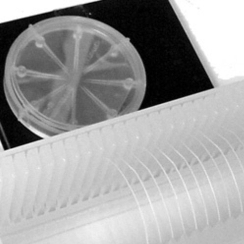

Al2O3- Sapphire Wafer, R Plane, 2" dia x 0.5mm, 1sp
Fearures:
- R plane -- (1-102) orientation sapphire wafer is being used as a superconductor substrate due to less mis-matched lattice and stable chemical and physical properties.
- Wafer size: 2" dia x 0.4 - 0.5 mm thickness
- (1-102) Rplane orientation +/-0.5 Deg
- Polished surface: Wafer surface is EPI polished via a special CMP procedure
- One side polished
- Package: Each wafer is packed in 1000 class clean room with 100 grade plastic bag with wafer container
- Precaution: R plane sapphire wafer is easy to cleave compared with C plane's. Please handle it with a care
Typical Properties:
- Crystal Structure: Hexagonal. a=4.758 Angstroms c=12.99 Angstroms
- Melting Point: 2040 degree C
- Density: 3.97 gram/cm2
- Growth Technique: CZ
- Crystal Purity: >99.99%
- Hardness: 9 ( mohs)
- Thermal Expansion: 7.5x10⁻⁶ (/ oC)
- Thermal Conductivity: 46.06 @ 0 oC, 25.12 @ 100 oC, 12.56 @ 400 oC ( W/(m.K) )
- Dielectric Constant: ~ 9.4 @300K at A axis ~ 11.58@ 300K at C axis
- Loss Tangent at 10 GHz: < 2x10⁻⁵ at A axis, <5 x10⁻⁵ at C axis

